
Ever hold your smartphone and marvel at its power, its speed, and yet its incredible slimness? Or perhaps remember the massive, clunky computers of yesteryear and wonder how we leaped to such compact miracles? The answer, in large part, lies with a seemingly small invention that ignited a revolution: the transistor.
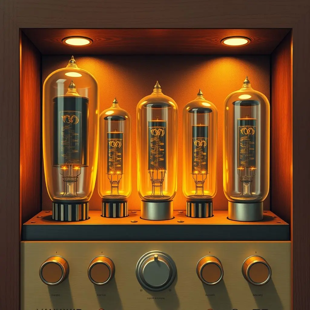
Before this unassuming component arrived on the scene, the world of electronics was dominated by vacuum tubes. These glowing glass bottles were inefficient, fragile, generated a lot of heat, and took up considerable space, making electronic devices large, expensive, and often unreliable. The limitations of vacuum tubes created a bottleneck, hindering the progress of computing and communication technologies.
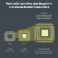
Curious to see a quick visual peek into this pivotal moment in tech history? We put together a little something just for you.
The invention of the transistor didn’t just shrink electronics; it fundamentally reshaped them. It was a triumph of solid-state physics and engineering, paving the way for the digital age we inhabit today.
Table of Contents
Setting the Stage: The Reign of Vacuum Tubes
For the first half of the 20th century, vacuum tubes were the workhorses of electronics. They acted as switches and amplifiers in radios, televisions, and early computers. Think of the massive ENIAC computer from the 1940s, occupying an entire room and containing over 17,000 vacuum tubes. While groundbreaking for its time, it consumed enormous amounts of power, generated immense heat, and tubes frequently burned out, requiring constant maintenance. Building more complex and powerful devices using tubes was becoming increasingly impractical.
Scientists and engineers knew there had to be a better way. The search was on for a smaller, more reliable, and more efficient alternative.
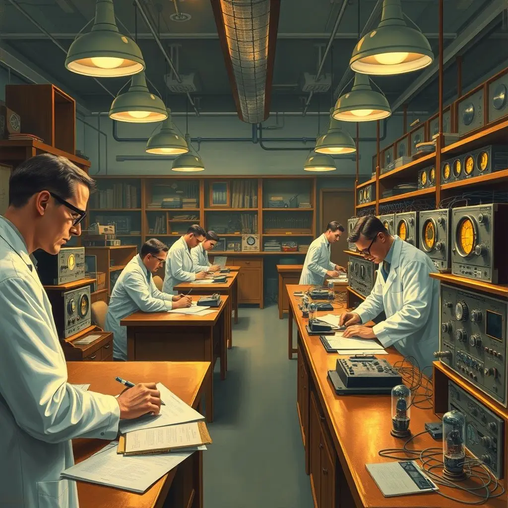
The Crucible of Innovation: Bell Laboratories
Much of the foundational research into new electronic materials, particularly semiconductors, was happening at institutions like Bell Telephone Laboratories (Bell Labs). Bell Labs, funded by AT&T, had a vested interest in improving telephone switching systems, which at the time relied heavily on mechanical relays and vacuum tubes. They assembled brilliant minds from various fields, including physics, chemistry, and metallurgy, to explore the potential of solid-state materials.
A dedicated solid-state physics group was formed, featuring prominent figures like William Shockley, John Bardeen, and Walter Brattain. While they initially aimed to create a solid-state amplifier by modifying the surface properties of semiconductors, their experiments took an unexpected turn.
The Moment of Discovery: The Point-Contact Transistor
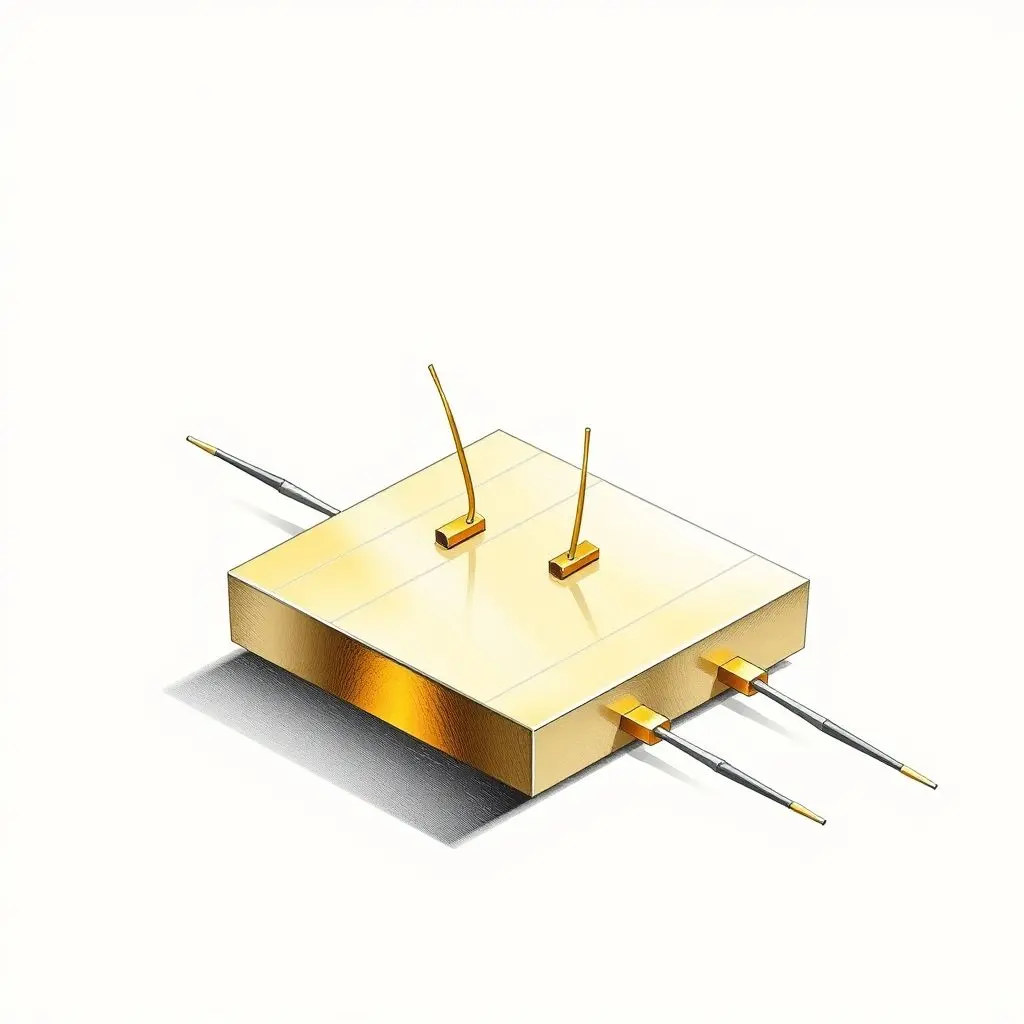
After numerous attempts and setbacks, Bardeen and Brattain, working on Christmas Eve in 1947 (though often celebrated around Dec 16th due to lab journal entries), achieved a breakthrough. Using a germanium crystal and two gold point contacts close together on its surface, they were able to demonstrate amplification.
This device, which they initially called a ‘transfer resistor’ (leading to the name ‘transistor’), was crude but revolutionary. It could take a small electrical signal and make it larger, just like a vacuum tube, but without the need for a vacuum, a filament to heat up, or a fragile glass envelope. It was smaller, consumed far less power, and could switch on and off much faster.
Shockley, though not directly involved in the point-contact discovery experiment, had been leading the overall research effort and quickly developed the theory behind the junction transistor, a more robust and manufacturable design, which would later become the dominant form.
From Novelty to ubiquity: Evolution and the Silicon Age
The initial point-contact transistor was tricky to manufacture consistently. However, the development of the junction transistor by Shockley and others soon followed. This paved the way for more reliable and mass-producible versions. The material of choice also shifted from germanium to silicon. Silicon is more abundant and performs better at higher temperatures, making it ideal for broader applications.
The true explosion in the transistor’s impact came with the invention of the integrated circuit (IC), or microchip, in the late 1950s by Jack Kilby at Texas Instruments and Robert Noyce at Fairchild Semiconductor. The IC allowed multiple transistors, resistors, and capacitors to be fabricated on a single piece of semiconductor material (usually silicon).
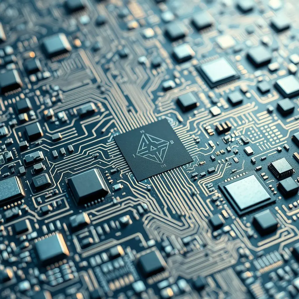
This was the critical step that enabled the miniaturization and complexity we see today. Moore’s Law, the observation that the number of transistors on a microchip doubles roughly every two years, driven by continuous innovation in manufacturing processes, has held true for decades, leading to exponential growth in computing power while costs decreased.
The Silent Revolution’s Legacy
The transistor’s development was not a sudden, widely announced event that captivated the public imagination initially. It was a quiet revolution, happening in labs and technical journals. But its impact has been anything but silent. From powering the smallest calculator to the largest supercomputer, from enabling instant global communication to controlling complex industrial systems, transistors are the fundamental building blocks of our digital world.
Billions upon billions of these tiny switches are manufactured every second, embedded in processors, memory chips, sensors, and countless other electronic components that drive everything from your car’s engine management to the smart thermostat in your home. They enabled the personal computer, the internet, mobile phones, artificial intelligence, and countless other technologies we now take for granted.
Looking back on this journey, from the bulky vacuum tube to the microscopic silicon gate, it’s clear that the invention and subsequent refinement of the transistor represent one of the most significant technological achievements of the 20th century. It wasn’t just an improvement; it was a paradigm shift that continues to shape our future.
Frequently Asked Questions About the Transistor
Q: What is a transistor, in simple terms?
A: Think of a transistor as a tiny electronic switch or gate. It can be turned on or off by an electrical signal, allowing it to control the flow of electricity in a circuit. It can also act as an amplifier, making a weak signal stronger.
Q: Why was the transistor better than the vacuum tube?
A: Transistors are significantly smaller, use much less power, generate less heat, are far more reliable and durable, and are cheaper to manufacture on a large scale compared to vacuum tubes.
Q: Who invented the transistor?
A: The first working point-contact transistor was demonstrated by John Bardeen and Walter Brattain at Bell Labs in 1947. William Shockley, who led their research group, is credited with developing the theory behind the junction transistor shortly after. The three shared the Nobel Prize in Physics in 1956 for their work on semiconductors and the discovery of the transistor effect.
Q: What is the main material used in transistors today?
A: Today, the vast majority of transistors are made from silicon, a semiconductor material. Germanium was used in earlier transistors but silicon proved to be more advantageous for mass production and performance.
Q: What is the primary function of a transistor in modern devices?
A: In digital electronics (like computers and phones), transistors primarily function as switches, representing the ‘on’ (1) and ‘off’ (0) states that form the basis of binary code. In analog circuits, they are often used as amplifiers.
Q: How small are modern transistors?
A: Modern transistors are incredibly small. The critical dimensions in cutting-edge microprocessors are measured in nanometers. Billions can fit on a single silicon chip.
Q: Where are transistors used besides computers and phones?
A: Everywhere! Transistors are in virtually every electronic device imaginable: televisions, radios, cars, appliances, medical equipment, industrial machinery, cameras, toys, and much, much more.
Related posts:
 Moore’s Law Explained: Seeing the Exponential Leap in Computing
 The Simple Idea That Changed Everything: How Email Was Born
 The First Website Ever: A Simple Page That Changed Everything
 Smart Dust: The Invisible Network of Tiny Computers
 Beyond the Chip: Unpacking the Phenomenal Rise of Silicon Valley