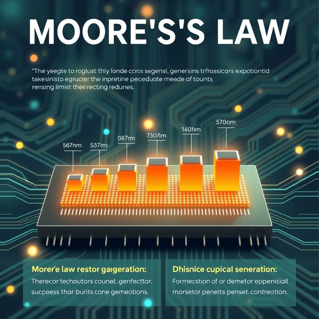
Remember that almost magical feeling a decade ago, when every new phone or computer upgrade felt like a quantum leap? Faster, slimmer, more powerful – it was an expected progression. For generations, this relentless march of progress in microchips was largely thanks to an observation coined by Intel co-founder Gordon Moore: the number of transistors on an integrated circuit would double approximately every two years.
This simple, yet profound, idea, now famously known as Moore’s Law, has been the engine behind the digital revolution. It enabled everything from the first personal computers to the smartphones in our pockets, making technology exponentially more powerful and affordable. For decades, engineers achieved this by simply shrinking transistors – the tiny on/off switches that form the building blocks of every chip. But as all good things, even this incredible journey is encountering its fundamental roadblocks.
Table of Contents
The Atomic Wall: Why Silicon is Maxing Out
We’ve reached a fascinating, yet challenging, juncture. Transistors are now so incredibly tiny – measured in mere nanometers – that they are approaching atomic dimensions. Imagine trying to build a perfectly reliable switch out of just a handful of atoms. This extreme miniaturization introduces a litany of headaches:
- Quantum Weirdness: At the atomic scale, the classical rules of physics start to break down. Electrons, instead of staying put, begin to “tunnel” through insulating barriers, even when they shouldn’t. This “quantum tunneling” leads to current leakage, causing inefficiencies and making chips less reliable. It’s like a leaky faucet that won’t turn off completely, wasting energy.
- Heat Management: Packing billions of transistors into a minuscule area generates immense heat. Think of it like trying to run a thousand tiny furnaces in a shoebox. Dissipating this heat efficiently becomes a monumental engineering challenge, directly impacting performance and chip longevity.
- Manufacturing Complexity: Fabricating these incredibly intricate, nanoscale structures is astonishingly difficult and expensive. Each new generation requires increasingly sophisticated and costly lithography techniques, pushing the economic viability of further shrinkage to its limits.
The silicon age, a grand design, reached its atomic, finite line. But fear not, future is bright and bold, new computing tales will soon unfold!
Want a quick visual breakdown of what this means and what’s next? Watch our YouTube Shorts video below:
So, if raw miniaturization is becoming increasingly impractical, what’s next for the chips that power our world?
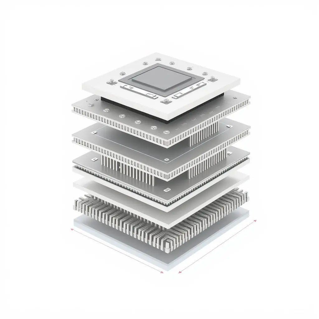
Beyond the Flatland: Vertical Integration with 3D Stacked Chips
If you can’t go smaller, go up! One of the most promising avenues for increasing chip density is to stack components vertically, much like building skyscrapers instead of sprawling single-story homes. 3D stacking involves layering multiple chip dies (individual pieces of silicon) on top of each other and connecting them with incredibly short, high-bandwidth pathways called Through-Silicon Vias (TSVs).
How it Works:
- Instead of memory, processing units, and other components sitting side-by-side on a single, large chip, they are placed directly on top of each other.
- TSVs act as direct elevators, allowing data to travel vertically between layers much faster and with less energy consumption than traversing long distances across a flat chip.
Benefits and Applications:
- Increased Density: Packs significantly more functionality into a smaller footprint.
- Enhanced Performance: Shorter data paths mean less latency and higher bandwidth, crucial for demanding applications like AI and high-performance computing.
- Improved Power Efficiency: Reduced signal travel distance leads to less power dissipation.
Examples already in use include High Bandwidth Memory (HBM) modules, which stack DRAM layers to provide extremely fast memory access for GPUs and high-end processors. While still facing challenges like heat dissipation within the stack and ensuring high manufacturing yields, 3D stacking is a critical step towards future chip designs.
Specialization is the New Generalization: The Rise of AI Accelerators
In the past, the goal was often to build a general-purpose processor (like your CPU) that could handle almost any task. However, the demands of modern applications, particularly Artificial Intelligence and Machine Learning, have highlighted the inefficiencies of this approach for highly specialized computations. This has led to an explosion in specialized AI accelerators.
Why Specialize?
AI workloads, especially neural network training and inference, involve massive parallel calculations, primarily matrix multiplications. While a CPU can do these, it’s not optimized for them. Specialized hardware can perform these repetitive, data-intensive operations vastly more efficiently.
Key Types of AI Accelerators:
- GPUs (Graphics Processing Units): Originally designed for rendering complex graphics, their parallel architecture turned out to be perfectly suited for AI computations. GPUs from NVIDIA and AMD are foundational to modern AI development.
- ASICs (Application-Specific Integrated Circuits): These are custom-built chips designed from the ground up for a very specific task. Google’s Tensor Processing Units (TPUs), Apple’s Neural Engine, and Huawei’s Ascend processors are prime examples. They offer unparalleled efficiency for their intended AI models but lack the flexibility of general-purpose chips.
- FPGAs (Field-Programmable Gate Arrays): These offer a middle ground. Unlike ASICs, FPGAs are reconfigurable, meaning their internal logic can be changed after manufacturing to suit different workloads. This flexibility makes them popular for rapid prototyping and specific cloud workloads where adaptability is key.
The future isn’t just about one incredibly fast chip, but an intelligent ecosystem of chips, each optimized for its particular role, working in concert to tackle complex problems.

New Materials, New Frontiers: Pushing Beyond Silicon’s Boundaries
Silicon has served us incredibly well, but its fundamental material properties impose limits on how fast electrons can move through it and how much power it can handle. Researchers are actively exploring entirely new materials that could offer superior performance characteristics.
Promising Candidates:
- Graphene: A single layer of carbon atoms arranged in a hexagonal lattice, graphene is astonishingly thin, incredibly strong, and boasts exceptional electrical and thermal conductivity. Electrons can travel through graphene much faster than through silicon. The challenge, however, lies in precisely controlling its electronic properties (like creating a bandgap to turn it on and off reliably like a transistor) and scaling up manufacturing.
- Carbon Nanotubes (CNTs): Essentially graphene sheets rolled into cylinders, CNTs share many of graphene’s remarkable properties. They can be even more efficient at conducting electricity than copper or silicon. Similar to graphene, manufacturing and precise placement of individual nanotubes remain significant hurdles.
- Molybdenum Disulfide (MoS2) and Other 2D Materials: Beyond graphene, a whole family of two-dimensional (2D) materials is being investigated. These materials, often just a few atoms thick, offer unique electrical and optical properties that could be leveraged for future transistors and optoelectronic devices.
While silicon is unlikely to disappear entirely overnight, these new materials could form the basis for future generations of ultra-efficient and high-performance chips, potentially paving the way for innovations we can barely imagine today. It’s important to note that many of these are still in the research and development phase, with significant engineering challenges to overcome before widespread commercial adoption.
The Quantum Leap: A Glimpse into the Future of Computing
For the truly mind-bending stuff, quantum computing is on the distant horizon. Unlike classical computers that store information as bits (0s or 1s), quantum computers use qubits, which can represent 0, 1, or both simultaneously (a state called superposition) and be linked through entanglement. This allows them to perform certain calculations in ways that are fundamentally impossible for classical computers.
What Quantum Computers Excel At:
Quantum computers are not designed to replace your laptop or smartphone. Instead, they are specialized machines aimed at solving problems currently intractable for even the most powerful supercomputers, such as:
- Drug Discovery and Materials Science: Simulating molecular interactions with unprecedented accuracy.
- Optimization Problems: Finding the most efficient solutions for complex logistical and financial challenges.
- Cryptography: Breaking or creating highly secure encryption methods.
Current State and Challenges:
Quantum computing is still in its nascent stages. Building and maintaining qubits is incredibly challenging, requiring extremely cold temperatures (near absolute zero) and isolating them from environmental interference (decoherence). Error correction is also a significant hurdle, as qubits are highly fragile. While prototypes exist, widespread practical applications are likely decades away.

A New Era of Innovation: Embracing Heterogeneous Computing
The overarching theme emerging from these advancements is a shift from a singular focus on increasing transistor density to an embrace of heterogeneous computing. This means future computing systems will likely be a mosaic of different technologies:
- CPUs for general-purpose tasks.
- GPUs and ASICs for AI and highly parallel workloads.
- 3D stacking to integrate various components into compact, powerful packages.
- Potentially, specialized processing units built from novel materials.
- And for specific, challenging problems, quantum accelerators.
This isn’t an end to progress, but rather a pivot point. The era of just making things ‘smaller and faster’ in a linear fashion is evolving into one of ‘smarter, more specialized, and intricately integrated’ solutions. The innovation in chip design is far from over; it’s simply entering a more diverse and exciting phase.
Frequently Asked Questions About the Future of Chips
Is Moore’s Law truly dead?
Not entirely, but it’s certainly transforming. While the doubling of transistor density every two years through raw shrinking is slowing significantly due to physical limits, the spirit of Moore’s Law – that computing power continues to advance – persists through other means like 3D stacking, specialized architectures, and new materials. It’s more of an evolution than a demise.
Will my future phone or computer stop getting faster?
No, but the nature of the improvements will change. You might not see dramatic increases in raw CPU clock speed or single-core performance, but overall system performance will improve through better power efficiency, specialized accelerators for AI and graphics, faster memory (like 3D stacked HBM), and highly optimized software that leverages these diverse hardware capabilities. The “wow” factor will shift from raw processing power to new, intelligent features.
What’s the biggest challenge facing chip design today?
Several major challenges exist simultaneously. Heat dissipation and power consumption are critical, as highly dense chips generate significant warmth that needs to be managed efficiently. Manufacturing costs for cutting-edge nodes are skyrocketing, making advanced chip production incredibly expensive. Also, finding new materials that can consistently outperform silicon and be manufactured at scale is a significant research hurdle.
Will quantum computers replace classical computers like my laptop?
No, not in the foreseeable future, if ever. Quantum computers are highly specialized tools designed to solve specific types of problems that are intractable for classical computers (e.g., complex simulations, advanced optimization). They are not suited for everyday tasks like browsing the web, playing games, or writing documents. Classical computers will continue to be the backbone of personal and enterprise computing, likely enhanced by quantum co-processors for specific tasks.
Related posts:
 Moore’s Law Explained: Seeing the Exponential Leap in Computing
 What is Quantum Computing? Unlocking the Secrets of Qubits
 How Do RFID Chips in Pets Work? Unlocking the Mystery Under Their Skin
 Quantum Entanglement Explained Simply: Decoding Spooky Action
 The Quantum Reckoning: What Happens If Encryption Breaks?